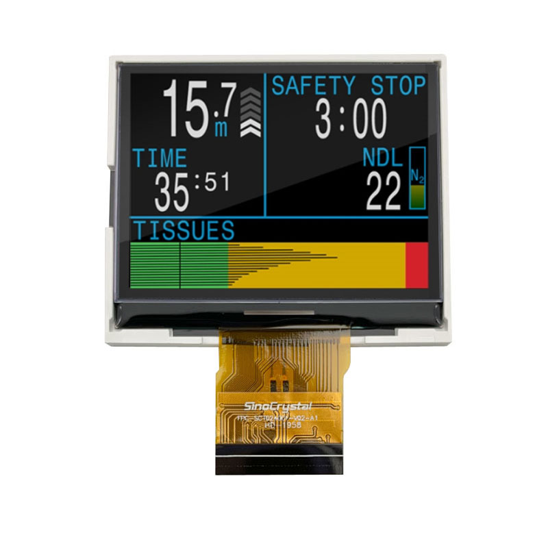


2.4英寸TFT,480 * 234,8bit RGB接口,OTA5182A IC
SCT024001-V02 is a 2.4” TFT LCD Display with 480*234 resolution, it built in with OTA5182A IC, and it supports 8bit RGB interface, 40 PIN, 6 o’clock View direction.
DESCRIPTION
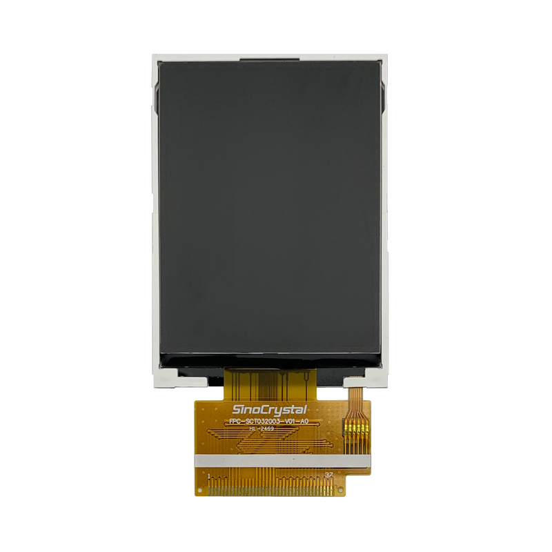
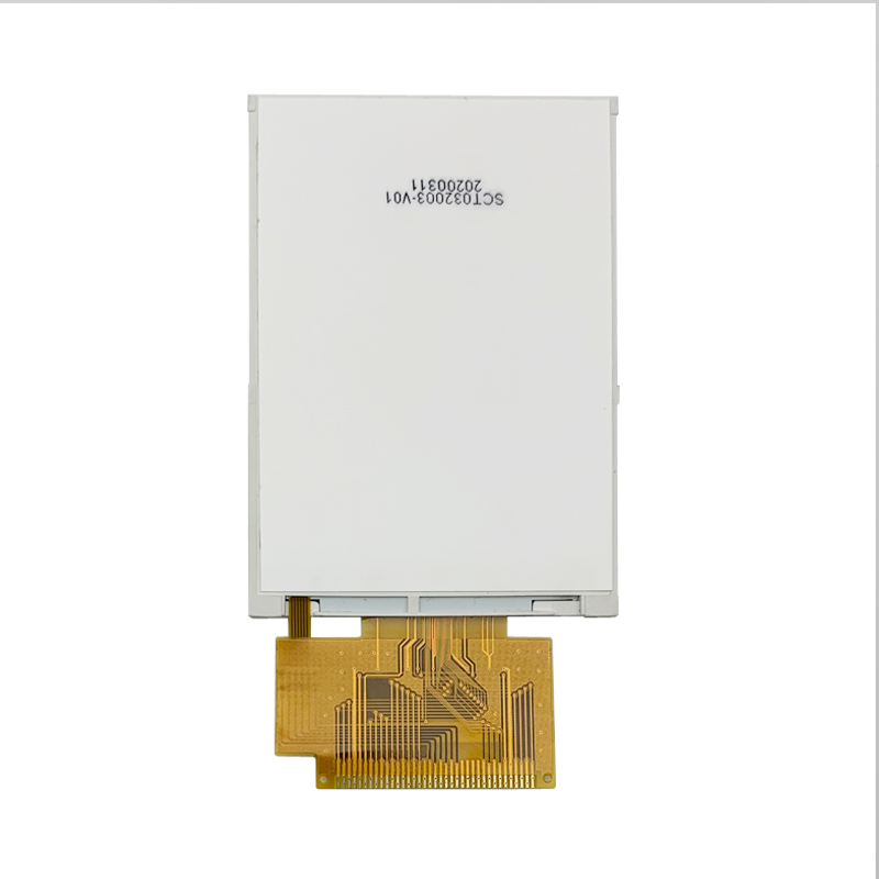
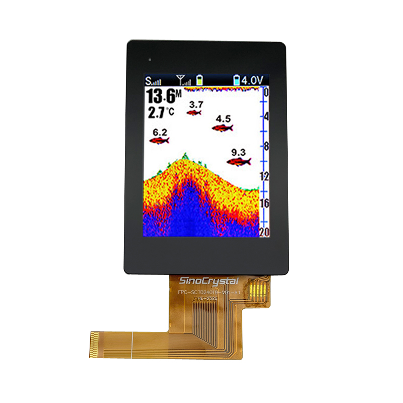
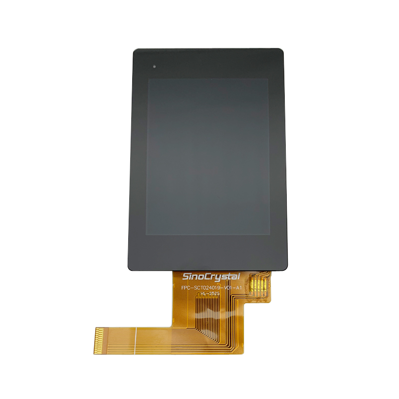
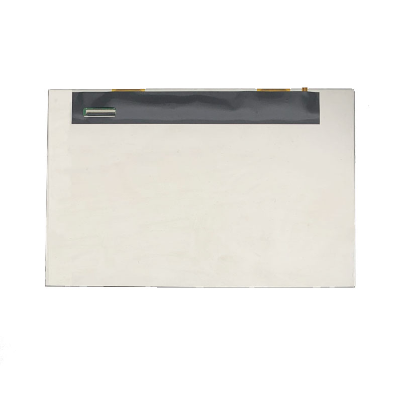
Drawing

General Specification
| Item | Nominal Dimension | Unit |
|---|---|---|
| Dot Matrix | 480 x 234 | Dots |
| Module Size ( W×H×T ) | 55.2 x 47.55 x 2.8 | mm. |
| Active Area ( W×H ) | 48.0 x 35.685 | mm. |
| Pixel arrangement | RGB Delta Stripe | mm. |
| Color depth | 262K(MAX) | colors |
| Interface | 8 bit RGB | – |
| Driving IC Package | COG | – |
| Operating temperature | -20 ~70 | ºC |
| Storage temperature | -30~80 | ºC |
| LCD Type | a-Si TFT | – |
| LCD Mode | TN/Normal White | – |
| Backlight Type | LED x 2 | PCS |
Interface Definition
| Pin No | Pin Symbol | Type | Description |
|---|---|---|---|
| 1-2 | NC | ||
| 3 | C1N | – | Pins to connect capacitors for power circuitry |
| 4 | C2N | – | Pins to connect capacitors for power circuitry |
| 5 | C1P | – | Pins to connect capacitors for power circuitry |
| 6 | C2P | – | Pins to connect capacitors for power circuitry |
| 7–9 | NC | ||
| 10 | VDD3 | – | Intermediate voltage for charge pump |
| 11 | VDD_25V | – | Intermediate voltage for charge pump |
| 12 | AGND | – | Power ground |
| 13 | NC | ||
| 14 | VCAC | – | Intermediate voltage for charge pump |
| 15 | C3P | – | Pins to connect capacitors for power circuitry |
| 16 | C3N | – | Pins to connect capacitors for power circuitry |
| 17 | DRV | – | Gate signal for the power transistor of the boost converter |
| 18 | FB | – | Main boost regulator feedback input |
| 19 | LEDK | – | LED backlight Cathode |
| 20-21 | NC | ||
| 22 | LEDA | – | Supply voltage for LED backlight Anode |
| 23 | GND | – | Power ground |
| 24 | VDD | – | Power supply for analog(1.8V-3.6V) |
| 25 | VSYNC | H/L | Frame synchronizing |
| 26 | HSYNC | H/L | Line synchronizing |
| 27 | DCLK | H/L | Data clock |
| 28-35 | D0-D7 | H/L | Data input |
| 36 | SDA | H/L | Serial data input |
| 37 | SCL | H/L | Serial clock input |
| 38 | CSB | H/L | Serial chip select, Low enable |
| 39 | NC | ||
| 40 | GRB | H/L | Global reset pin |